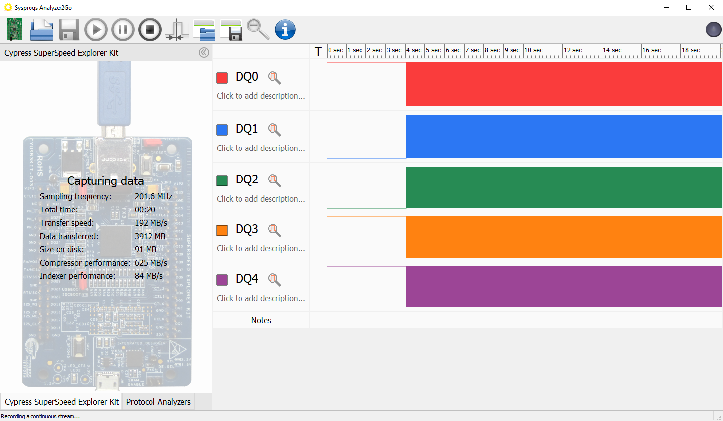
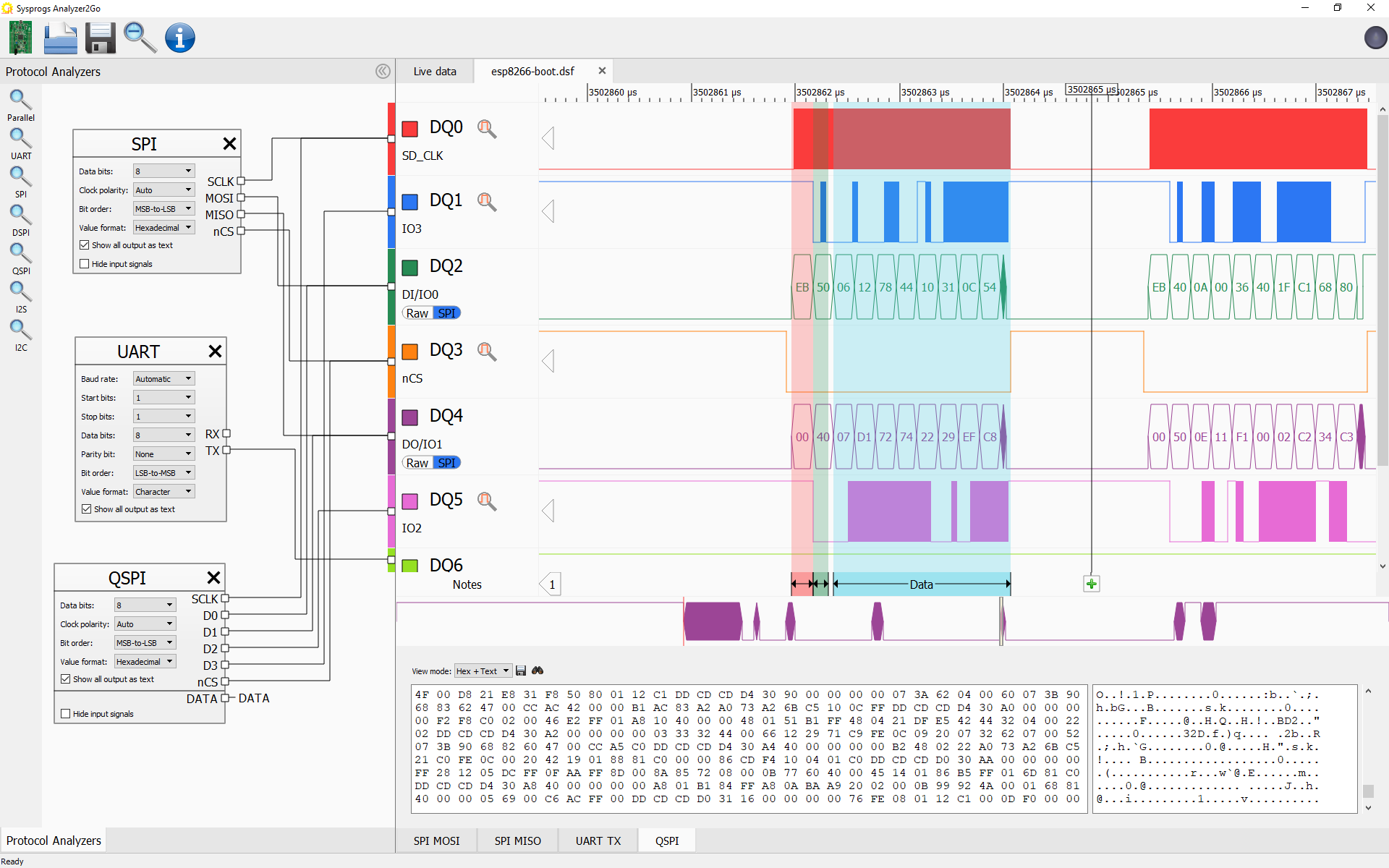
Today we are proud to announce the release of Analyzer2Go 2.0 – our product that turns development boards into powerful logic analyzers. This release adds support for the Cypress SuperSpeed Explorer Kit that is capable of streaming data to the computer over the ultra-fast USB 3.0 interface at >350MB/sec, resulting in reliable 200MHz sampling rate when using 8 channels or 100 MHz when using 16 channels. The SuperSpeed Explorer Kit is the perfect board to be used as a logic analyzer due to its highly programmable peripheral interface module and in this post I will explain to you how it works and how you can use it to add extremely fast connectivity to your designs.
Why not just use the CPU
Although modern embedded CPUs can run at impressive speeds, executing each instruction involves a lot of work. It needs to be fetched from memory, translated and executed. If the instruction involves accessing peripheral registers (e.g. to read data from the board’s ports), it might take even longer. If you try using a simple software loop to toggle one digital output on the super-fast STM32H7 running at 400 MHz, you will only observe around a 16 MHz output clock. Add on the delays necessary to handle various USB requests, respond to commands, count data, etc, and the CPU-only option for a fast interface quickly becomes nonviable.
That’s the exact reason why practically every microcontroller out there comes with a diverse portfolio of interface modules – SPI, UART, I2C, you name it. The Cypress engineers realizing the amount of data flying around when using USB 3.0 at maximum speeds went further and designed a General Programmable Interface Module (GPIF) that is not hardcoded to handle a specific protocol, but instead can be tweaked to do a bunch of simple actions at precisely each cycle of the internal 200 MHz clock, letting the main CPU spend 100% of the time orchestrating the transfers rather than endlessly moving data between registers.
Programming the GPIF
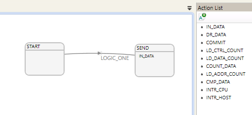
The GPIF module stands somewhere between an FPGA and a separate small CPU. It cannot be programmed to perform completely arbitrary calculations, however it can do one or more very basic operations on each cycle of its internal clock. Those operations include sampling the input pins, updating various counters, comparing data with predefined values and pushing data into the pre-configured DMA channel that goes straight into the USB3 module. The GPIF is programmed as a state machine using GPIF II Designer – a tool from Cypress. Once you lay out a set of states and define rules for switching between them, and also what to do in each state, it will generate a configuration vector that your firmware can load into GPIF at runtime.
Say you just want to sample the input bus each clock cycle and send it to USB. In this case you would need just 1 state (SEND) that will repeat forever and read data on each clock cycle: Toss in some basic initialization code to connect the GPIF output socket to a USB 3.0 endpoint and you’re good to go:
CyU3PDmaChannelConfig_t dmaCfg; CyU3PMemSet ((uint8_t *)&dmaCfg, 0, sizeof (dmaCfg)); dmaCfg.size = CY_FX_DMA_BUF_SIZE; dmaCfg.count = CY_FX_DMA_BUF_COUNT; dmaCfg.prodSckId = CY_U3P_PIB_SOCKET_0; dmaCfg.consSckId = CY_U3P_UIB_SOCKET_CONS_1; dmaCfg.dmaMode = CY_U3P_DMA_MODE_BYTE; dmaCfg.prodHeader = 0; dmaCfg.prodFooter = 0; dmaCfg.consHeader = 0; dmaCfg.prodAvailCount = 0; dmaCfg.notification = CY_U3P_DMA_CB_CONS_SUSP; dmaCfg.cb = GpifToUsbDmaCallback; CyU3PDmaChannelCreate (&glDmaChHandle, CY_U3P_DMA_TYPE_AUTO, &dmaCfg); |
Of course this basic example doesn’t check for buffer overruns, so you could add another state that won’t be sending any data. Configure GPIF to enter it as soon as the DMA is not ready and get back to sending once the DMA is available again. The beauty of it is that the transition conditions are checked on every clock cycle with no exceptions, no pipeline delays and no interrupts. The conditions can be reasonably complex like DMA_RDY_TH0 & !DATA_CNT_HIT (which means “DMA on channel 0 is ready and the internal data counter has not expired yet”) and they will still take exactly 1 clock cycle to evaluate. The GPIF module includes 2 counters that can be configured to count up/down, a few internal registers that can be loaded with data and a comparator. So even if you want to do something tricky, like wait for a specific value to appear on the bus and then send a massive load of data in or out, after a few iterations you can figure out a state machine that will handle that.
For the logic analyzer we used a slightly modified version of the above-pictured state machine that also included double-buffering, then we ensured that no data is lost by watching for the GPIF overrun interrupts and recording & analyzing a few test signals. The GPIF lived up to the expectations, capturing a frame every clock cycle and sending it out via USB with no losses on the way.
The main CPU
The Cypress microcontroller on the SuperSpeed Explorer Kit board features a fast ARM-based CPU. Although it’s free from the burden of physically moving the data between GPIF and USB3, it is actively used to setup various peripherals before they can work together on their own. The typical firmware for the CYUSB301X controller does the following steps:
- Configures clocks for all components.
- Creates the main thread (the Cypress SDK includes a basic RTOS).
- Registers the USB descriptors with the SDK so that the device can identify itself to the USB host.
- Loads the configuration vector generated by the GPIF designer.
- Connects GPIF with the USB3 module using the DMA sockets.
- Handles high-level events like “connected to a USB host” or “received a request over the control endpoint”.
The framework is actually pretty flexible, e.g. you can load different configuration vectors to the GPIF based on custom USB requests received from your PC program, or you can change the way the device responds to various USB requests. In our logic analyzer design we ended up dynamically loading a GPIF configuration based on the capture settings selected in the client program and the Cypress SDK did the job perfectly.
The PC Side
Although the GPIF module on the Super Speed Explorer board solves the problem of quickly capturing massive amounts of data, it creates another problem – compressing and indexing a 200MB/s data stream in real time isn’t easy even on a modern CPU. We have solved this by splitting the compression load between all available CPU cores and using special techniques to allocate vast amounts of RAM even beyond the regular 2GB per process limit to buffer the data in case the compressor cannot keep up.
Capturing even a few minutes at 200 million samples per second can quickly produce countless gigabytes of data, and you don’t want to look through all of it each time you are looking at a high-level picture before you zoom in to the area of interest where you can actually see individual pulses. To tackle this, we have further optimized the format used by Analyzer2Go to store the captured data. Instead of just storing the entire data set, Analyzer2Go splits signal data into chunks. Each chunk is virtually zoomed out until adjacent pulses shrink below pixel boundaries, merging them into a special “multiple pulses” record and producing a much smaller preview chunk. Adjacent preview chunks are then merged together until they get roughly the same size and the process is repeated exponentially, producing minimal overhead. Depending on the zoom level you are currently using, Analyzer2Go will automatically pick a chunk level with sufficient precision, so even if your captured data file is gigabytes long and the signal varies from extremely slow to extremely fast, looking around and zooming will be still instantaneous.
Try it out
You can download Analyzer2Go from our download page. It will automatically install the necessary drivers for your Super Speed Explorer Kit (if you don’t have them already) and will program the firmware into the RAM, so you can start taking your readings right away.
If you have any feedback about Analyzer2Go, don’t hesitate to write us an email, or use the contact form.
